What a Viral Antenna Post Teaches Us About Good IoT Prototyping

An unassuming photo of a test PCB triggered exactly what good technical content often does on LinkedIn: attention, pushback, and an instructive debate about IoT prototyping. Anyone who wants to learn fast in hardware development should test multiple ideas in parallel rather than waiting for successive prototype iterations. But especially in antenna design, that approach can become problematic.
Summary
- Parallel prototyping can help in hardware development to test multiple design approaches against each other in a short time and shorten development cycles.
- In antenna design, test setups are particularly sensitive, because antenna geometry, ground plane, component placement, and environment directly influence the result.
- For reliable conclusions, a clear distinction must be made between early functional screening and a proper RF or antenna evaluation under realistic conditions.
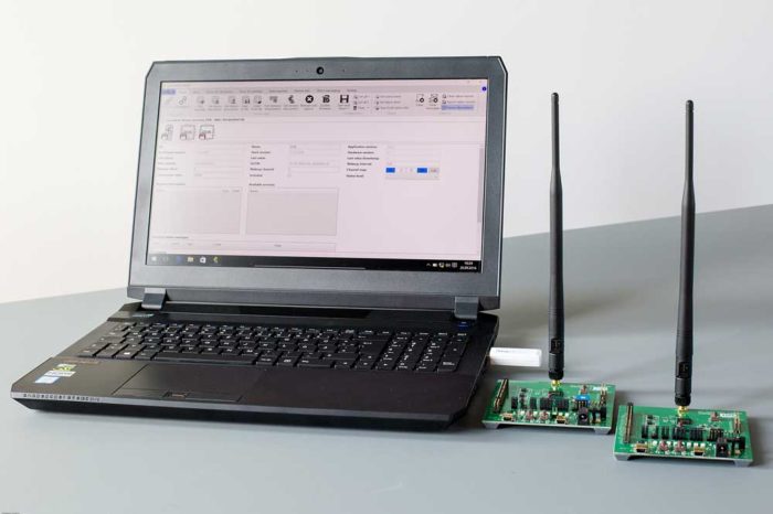
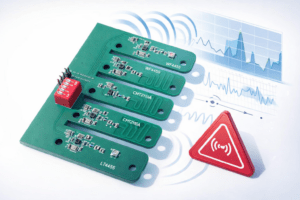
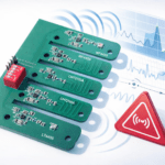
The image was posted by Peter Grinalds, CEO of Grinalds Solutions in Ohio, USA. What it showed: an RF transmitter test board with various antenna and chip combinations on a single PCB. Grinalds explained that in this particular project, the goal had not been to characterize radiation patterns or final RF performance. Instead, his team had wanted to quickly compare different combinations of RF transmitter chipsets, antenna geometries, and matching networks during an early project phase. The photo shows five PCB sections: two featuring the WF4455, one with the CMT2110A, and two with the LT4455 – each paired with a different antenna geometry. One board, multiple parallel experiments, less time lost, lower costs, faster decisions.
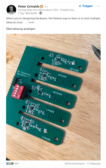
Screenshot of Peter Grinalds’ LinkedIn post: The RF test board with multiple antenna and chip variants sparked an intense debate about rapid prototyping, methodological limitations, and the pitfalls of antenna design.
As a principle for early-stage prototyping, the approach is understandable. But to many experts, the photo told a different story.
Criticism from the experts
Numerous antenna and RF engineers weighed in on the comments. The mood was anything but divided: while generalists and commentators from the manufacturing space largely praised the approach, the RF expert community was almost unanimously critical.
The most precise analysis came from Harald Naumann, winner of the 5G NTN Antenna Award and one of the most authoritative voices in the thread. He identified several concrete flaws in the setup:
- First, the antennas placed side by side interfere with each other – much like speakers positioned too close together that acoustically disrupt one another. The spacing falls below the critical minimum of lambda/4 (one quarter of the wavelength) required in RF engineering, and all antennas point in the same direction. The result: each antenna no longer “sees” its own environment, but one distorted by its neighbours. Katerina G., Senior Antenna Engineer from Sweden, summed it up in the comments: the board effectively behaves like an antenna array – a system of multiple antennas intentionally working together – rather than independent test candidates.
- Second, Naumann is critical of the antenna geometry: the structures appear to be L-antennas, whereas F-antennas would have been the better choice. The difference lies, simply put, at the feed point – the location where the signal is fed into the antenna. F-antennas inherently provide 50 ohms of impedance there, which matches the standard of most RF chips. L-antennas do not, which complicates impedance matching and distorts measurement results.
- Third, the ICs under test operate in different frequency ranges. Since the optimal antenna length depends directly on frequency – the lower the frequency, the longer the antenna needs to be – the same antenna structures simply do not suit all chips equally well. A fair comparison is therefore compromised from the outset.
- Fourth, the ground plane in the test setup is simply too small. PCB trace antennas are highly sensitive to the size and geometry of the ground plane – the copper area on the board that acts as a counterweight to the antenna and plays a major role in determining its electrical behaviour. An undersized ground plane significantly alters the antenna’s input impedance, with a direct consequence: the so-called “hand effect”, meaning extreme sensitivity to the influence of the user or surrounding environment during operation.
An antenna is more than its trace pattern
This gets to the real core of the problem. In PCB antennas, it is not only the visible trace that matters. The board’s ground plane, the position on the PCB, neighbouring structures, and ultimately even the enclosure are all integral parts of the overall system.
Anyone placing different antenna variants side by side on a shared test board is already altering the conditions under which those antennas operate. If one of the variants is later transferred to a separate board or into the target enclosure, the electrical situation is no longer the same. Yury Ilin, Senior Embedded Hardware Design Engineer from Canada, made a particularly sobering point in the thread: even switching PCB manufacturers changes antenna behaviour through differing material properties – to say nothing of VNA tuning and enclosure integration.
What the community suggested: separable boards as a compromise
Several engineers proposed a more pragmatic middle ground: designing the variants to be separable using mouse bites or V-scoring. This allows individual sections to be snapped off after an initial overview and tested separately under more realistic conditions – without waiting for an entirely new manufacturing run. This approach would at least have mitigated the coupling problem and enabled cleaner individual measurements per variant.
Grinalds himself responded calmly. The board had never been intended for proper antenna characterisation, but only for an early shortlist of chipsets and antenna styles. For the actual RF evaluation, a dedicated board had subsequently been built inside the final enclosure, with proper VNA tuning and matching.
The real value of the debate: speed versus accuracy
That is precisely where the value of this discussion lies – and it goes well beyond a single LinkedIn post. Grinalds’ contribution was not interesting because everything was done correctly. It was interesting because it revealed a genuine trade-off in hardware development: speed versus accuracy.
In early development phases, it is entirely legitimate to quickly eliminate hypotheses. But the closer a prototype gets to physically sensitive areas such as RF, antennas, or EMC, the greater the risk that the test setup itself distorts the results – and creates false confidence in the process.
What IoT developers can take away
There is more to take away from this than just a viral LinkedIn moment. A prototype must answer a clearly defined question – and the test setup must not pre-empt or distort that answer. This is especially true in antenna design, where success depends not on the trace alone, but on the interplay of geometry, antenna type, impedance matching, ground plane size, enclosure, and real-world installation environment.
Good prototyping maximises learning. But only when a clean distinction is drawn between early functional screening and genuine performance evaluation. Those who blur that line – deliberately or under time pressure – risk iterating quickly in the wrong direction.
The real lesson from this post is therefore not that parallel prototyping is wrong. On the contrary: it is often the smart approach. But in RF and antenna design more than in most disciplines, a fast setup only saves time when it does not become a fast path to self-deception.
User Review
( votes)You may also like